ICs for Communications
Quad ISDN High Voltage Power Controller
QIHPC
PEB/F 2426 Version 1.1
Preliminary Data Sheet 06.99
DS 1
�•
PEB/F 2426
Revision History:
Current Version: 06.99
Previous Version:
None
Page
Page
(in previous (in current
Version)
Version)
Subjects (major changes since last revision)
For questions on technology, delivery and prices please contact the Infineon Technologies Offices
in Germany or the Infineon Technologies Companies and Representatives worldwide:
see our webpage at http://www.infineon.com
•
ABM®, AOP®, ARCOFI®, ARCOFI®-BA, ARCOFI®-SP, DigiTape®, EPIC®-1, EPIC®-S, ELIC®, FALC®54, FALC®56,
FALC®-E1, FALC®-LH, IDEC®, IOM®, IOM®-1, IOM®-2, IPAT®-2, ISAC®-P, ISAC®-S, ISAC®-S TE, ISAC®-P TE,
ITAC®, IWE®, MUSAC®-A, OCTAT®-P, QUAT®-S, SICAT®, SICOFI®, SICOFI®-2, SICOFI®-4, SICOFI®-4µC,
SLICOFI® are registered trademarks of Infineon Technologies AG.
ACE™, ASM™, ASP™, POTSWIRE™, QuadFALC™, SCOUT™ are trademarks of Infineon Technologies AG.
Edition 06.99
Published by Infineon Technologies AG i. Gr.,
SC,
Balanstraße 73,
81541 München
© Infineon Technologies AG i.Gr. 14/6/99.
All Rights Reserved.
Attention please!
As far as patents or other rights of third parties are concerned, liability is only assumed for components, not for
applications, processes and circuits implemented within components or assemblies.
The information describes the type of component and shall not be considered as assured characteristics.
Terms of delivery and rights to change design reserved.
Due to technical requirements components may contain dangerous substances. For information on the types in
question please contact your nearest Infineon Technologies Office.
Infineon Technologies AG is an approved CECC manufacturer.
Packing
Please use the recycling operators known to you. We can also help you – get in touch with your nearest sales
office. By agreement we will take packing material back, if it is sorted. You must bear the costs of transport.
For packing material that is returned to us unsorted or which we are not obliged to accept, we shall have to invoice
you for any costs incurred.
Components used in life-support devices or systems must be expressly authorized for such purpose!
Critical components1 of the Infineon Technologies AG, may only be used in life-support devices or systems2 with
the express written approval of the Infineon Technologies AG.
1 A critical component is a component used in a life-support device or system whose failure can reasonably be
expected to cause the failure of that life-support device or system, or to affect its safety or effectiveness of that
device or system.
2 Life support devices or systems are intended (a) to be implanted in the human body, or (b) to support and/or
maintain and sustain human life. If they fail, it is reasonable to assume that the health of the user may be endangered.
�PEB 2426
PEF 2426
Table of Contents
Page
1
1.1
1.2
1.3
Overview . . . . . . . . . . . . . . . . . . . . . . . . . . . . . . . . . . . . . . . . . . . . . . . . . . . .6
Features . . . . . . . . . . . . . . . . . . . . . . . . . . . . . . . . . . . . . . . . . . . . . . . . . . . . .7
Logic Symbol . . . . . . . . . . . . . . . . . . . . . . . . . . . . . . . . . . . . . . . . . . . . . . . . .8
Typical Applications . . . . . . . . . . . . . . . . . . . . . . . . . . . . . . . . . . . . . . . . . . . .9
2
2.1
2.2
Pin Descriptions . . . . . . . . . . . . . . . . . . . . . . . . . . . . . . . . . . . . . . . . . . . .11
Pin Configuration
(top view) . . . . . . . . . . . . . . . . . . . . . . . . . . . . . . . . . . . . . . . . . . . . . . . . . . .11
Pin Definitions and Functions . . . . . . . . . . . . . . . . . . . . . . . . . . . . . . . . . . .12
3
3.1
3.2
3.3
3.4
3.5
Functional Description . . . . . . . . . . . . . . . . . . . . . . . . . . . . . . . . . . . . . . .14
Functional Block Diagram . . . . . . . . . . . . . . . . . . . . . . . . . . . . . . . . . . . . . .14
Biasing Circuit . . . . . . . . . . . . . . . . . . . . . . . . . . . . . . . . . . . . . . . . . . . . . . .15
Line Feed Control Circuit . . . . . . . . . . . . . . . . . . . . . . . . . . . . . . . . . . . . . . .16
Line Current Control Circuit . . . . . . . . . . . . . . . . . . . . . . . . . . . . . . . . . . . . .17
Relays Driver Circuit . . . . . . . . . . . . . . . . . . . . . . . . . . . . . . . . . . . . . . . . . .18
4
4.1
4.2
4.3
4.4
Application Hints . . . . . . . . . . . . . . . . . . . . . . . . . . . . . . . . . . . . . . . . . . . .19
Resistor RS1..4 . . . . . . . . . . . . . . . . . . . . . . . . . . . . . . . . . . . . . . . . . . . . . .19
Resistor RF . . . . . . . . . . . . . . . . . . . . . . . . . . . . . . . . . . . . . . . . . . . . . . . . .19
Capacitor CS1..4 . . . . . . . . . . . . . . . . . . . . . . . . . . . . . . . . . . . . . . . . . . . . .19
Protection Circuitry . . . . . . . . . . . . . . . . . . . . . . . . . . . . . . . . . . . . . . . . . . .20
5
Operational Description . . . . . . . . . . . . . . . . . . . . . . . . . . . . . . . . . . . . . .21
6
6.1
6.2
6.3
6.4
6.5
Electrical Characteristics . . . . . . . . . . . . . . . . . . . . . . . . . . . . . . . . . . . . .23
Absolute Maximum Ratings . . . . . . . . . . . . . . . . . . . . . . . . . . . . . . . . . . . . .23
AC/DC-Characteristics . . . . . . . . . . . . . . . . . . . . . . . . . . . . . . . . . . . . . . . . .24
Operating Range . . . . . . . . . . . . . . . . . . . . . . . . . . . . . . . . . . . . . . . . . . . . .24
Static Thermal Resistance . . . . . . . . . . . . . . . . . . . . . . . . . . . . . . . . . . . . . .24
Testing the Electrical Parameters . . . . . . . . . . . . . . . . . . . . . . . . . . . . . . . .26
7
Package Outlines . . . . . . . . . . . . . . . . . . . . . . . . . . . . . . . . . . . . . . . . . . . .30
Preliminary Data Sheet
3
06.99
�PEB 2426
PEF 2426
List of Tables
Table 1
Table 2
Table 3
Table 4
Page
Pin Definitions and Functions . . . . . . . . . . . . . . . . . . . . . . . . . . . . . . .
Thermal Detector Threshold Levels . . . . . . . . . . . . . . . . . . . . . . . . . . .
Function Table for Controlling One Line . . . . . . . . . . . . . . . . . . . . . . .
DC Characteristics . . . . . . . . . . . . . . . . . . . . . . . . . . . . . . . . . . . . . . . .
Preliminary Data Sheet
4
12
15
17
25
06.99
�PEB 2426
PEF 2426
List of Figures
Figure 1
Figure 2
Figure 3
Figure 4
Figure 5
Figure 6
Figure 7
Figure 8
Figure 9
Figure 10
Figure 11
Figure 12
Figure 13
Figure 14
Figure 15
Page
Logic Symbol . . . . . . . . . . . . . . . . . . . . . . . . . . . . . . . . . . . . . . . . . . . . . .8
16-Line Card Application with DELPHI and QUAD-U . . . . . . . . . . . . . . .9
System integration . . . . . . . . . . . . . . . . . . . . . . . . . . . . . . . . . . . . . . . . .10
Pin Configuration . . . . . . . . . . . . . . . . . . . . . . . . . . . . . . . . . . . . . . . . . .11
Functional Block Diagram . . . . . . . . . . . . . . . . . . . . . . . . . . . . . . . . . . .14
Delay time tOC as a function of the value of CS1..4 (typical values). . .19
Proposal for a Protection Circuitry . . . . . . . . . . . . . . . . . . . . . . . . . . . . .20
Circuit with “LT Power Source Test Loads” . . . . . . . . . . . . . . . . . . . . . .21
Simultaneous Power Up Sequence . . . . . . . . . . . . . . . . . . . . . . . . . . . .22
Supply Currents . . . . . . . . . . . . . . . . . . . . . . . . . . . . . . . . . . . . . . . . . . .26
Line Currents and Delay Time tOC . . . . . . . . . . . . . . . . . . . . . . . . . . . .27
DMOS-RON resistance . . . . . . . . . . . . . . . . . . . . . . . . . . . . . . . . . . . . .27
PF1..4, Logic Input Levels and NACK1..4, Logic Output Levels . . . . . .28
RDin1..8, Relay Driver Inputs and RDout1..8 Relay Driver Outputs . . .29
Test circuit for maximum DC-voltages, pulse voltages and impulse voltages on pins D1..429
Preliminary Data Sheet
5
06.99
�PEB 2426
PEF 2426
1
Overview
The Quad ISDN High Voltage Power Controller provides a power source for up to four
U-line interfaces. The power source to the device is a local battery or a centralized power
supply.
Each powered line is individually controlled and monitored by the device interface. Line
powering can be switched on or off by command. The QIHPC indicates, when the output
current is above a threshold for longer than the programmable time tOC. At a second
(higher) value the current is limited. The values of the current limitation and the
overcurrent indication threshold are defined with external resistors, the overcurrent
indication setup delay is selected by external capacitances.
The status information of each line (acknowledge of requested power feed) is returned
to the system. The status information enables an easy detection of overloads and faults
and a fast localization even on a large system.
The integrated intelligent chip temperature control guards the QIHPC in case of
overloads.
Additionally eight drivers for external relays and their control logic are integrated on the
QIHPC. These relay drivers provide open collector output stages with high current
capability.
Preliminary Data Sheet
6
06.99
�Quad ISDN High Voltage Power Controller
QIHPC
PEB 2426
Version 1.1
1.1
SPT 170
Features
• ISDN Line Feed Supply Voltage up to 130 V
• Supplies power for up to four ISDN transmission
lines
• ETSI TS 102 080 compatible
• Separate Current Monitoring and Limiting for each
line
• Current Limiting Level can be programmed by an
external resistor
P-MQFP-44
• Overcurrent indication threshold can be programmed with external resistors
independently from the current limitation.
• The overcurrent indication setup delay can be programmed by external capacitors,
separately for each line
• Intelligent Chip Temperature Control
• Automatically switching off lines in current limitation when expecting over temperature
problems
• Automatically switching off all four lines in case of real overtemperature
• Integrated Relay Drivers and Relay Driver Controlling for eight relays
• Optimized for working in conjunction with PEB 24901 (DFE-T), PEB 24911 (DFE-Q),
and PEB 2491 (QUAD-U)
• Small P-MQFP-44 Package
• Reliable 170 V Smart Power Technology
Type
Package
PEB 2426
P-MQFP-44
Preliminary Data Sheet
7
06.99
�PEB 2426
PEF 2426
1.2
Logic Symbol
•
Relay Driver
input pins
Relay Driver pins
RDin1 . . . RDin8
Figure 1
D1
D2
D3
D4
QIHPC
VILF
S1 . . . S4
CS1 . . . CS4
Current
Sensing
Capacitor low
pass filter
PF1
PF2
PF3
PF4
Power Feed
Control Pins
Battery
Voltage
Power Feed
VDD
GND
NACK1
NACK2
NACK3
NACK4
Power Feed
Status Pins
RDout1 . . . RDout8
RFpos RFneg
Current
Sensing
Logic Symbol
Preliminary Data Sheet
8
06.99
�PEB 2426
PEF 2426
1.3
Typical Applications
The QIHPC is an integrated power controller especially designed for feeding two-wire
ISDN-transmission lines. Four U interface lines can be powered by one QIHPC.
PCM
Highway
test unit
1
Sign.
2
QUAD-U
IOM-2
DELPHI-LC
PEB 20570
PEB 2491
3
4
µC-Bus
Q-IHPC
PEB 2426
RAM
Figure 2
µC
16-Line Card Application with DELPHI and QUAD-U
Figure 3 gives general overview of the system integration of the QIHPC.
Because of integrated “pull-down current-sinks” on the input pins PF1..4 and RDin1..8 only
connections to VDD are necessary to switch on power feeding to the lines or to switch on
the relay drivers. When power feeding to a line is switched on, and this line is in a normal
feeding condition (current less than 50 mA), then the QIHPC shows a resistive
connection from Dx to Sx. Dx and Sx are the drain and source of the integrated DMOStransistor of channel x. The resistance value (DMOS-Ron) is typically 1.4 Ω with a total
tolerance of about +/- 0.35 Ω.
Preliminary Data Sheet
9
06.99
�PEB 2426
PEF 2426
•
Uk0
Channel1
AC-Path
Channel 1
VDD
VDD
OVP1
Uk0
Channel2
AC-Path
Channel 2
RDin1 . . . RDin8
RDout1 . . . RDout8
VDD
VDD
VDD
D1
OVP2
Uk0
Channel3
PF1
PF2
PF3
PF4
D2
D3
AC-Path
Channel 3
QIHPC
D4
NACK1
NACK2
NACK3
NACK4
VILF
VILF
OVP3
GND
S1 . . . S4
CS1 . . . CS4
RS1..4
Uk0
AC-Path
Channel 4
RFneg
CS1..4
4∗2Ω
Channel4
RFpos
4 ∗ 220 nF
VILF
RF
1700 Ω
VILF
OVP4
Figure 3
System integration
•
Preliminary Data Sheet
10
06.99
�PEB 2426
PEF 2426
Pin Descriptions
2.1
Pin Configuration
(top view)
RDin4
RDout4
RDout3
RDout2
RDout1
VDD
RDout5
RDout6
RDout7
RDout8
RDin8
2
RDin7
RDin6
RDin5
GND
D4
S4
CS4
CS3
S3
D3
GND
RFpos
RFneg
GND
PF1
PF2
PF3
PF4
NACK1
NACK2
NACK3
NACK4
RDin3
RDin2
RDin1
GND
D1
S1
CS1
CS2
S2
D2
VILF
Figure 4
Pin Configuration
Preliminary Data Sheet
11
06.99
�PEB 2426
PEF 2426
2.2
Pin Definitions and Functions
•
Table 1
Pin Definitions and Functions
Pin No. Symbol Input (I)
Function
Output (O)
28
VDD
Supply
Positive Supply Voltage, referred to GND.
Operating Voltage Range from 3.0 V to 6.0 V.
3
12
19
37
GND
Supply
Ground
44
VILF
Supply
ISDN Line Feed Voltage, referred to GND.
Operating Voltage Range from -130 V to -30 V.
38
43
13
18
D1
D2
D3
D4
O
Drain Connections of the Output Transistors
of Channels 1..4.
These pins have to be connected (via external
resistors) to ISDN lines a (ring) of channels 1..4.
1
2
RFpos
RFneg
O
Current limitation of Channels 1..4.
These pins have to be connected to an external
resistor RF. RF and RS1..4 are defining the output current
limit for all four lines.
39
42
14
17
S1
S2
S3
S4
O
Overcurrent indication threshold.
These pins have to be connected via external resistors
RS1..4 to VILF defining the overcurrent indication
threshold of each line individually.
40
41
15
16
Cs1
Cs2
Cs3
Cs4
O
External capacitors defining tOC-delays of
Channels 1..4.
These pins have to be connected via external
capacitors to VILF defining the overcurrent indication
delay.
4
5
6
7
PF1
PF2
PF3
PF4
I
Power Feed Signal of Channels 1..4.
Logic high on PF1..4 switches on the power feeding to
the line of channel 1..4.
8
9
10
11
NACK1
NACK2
NACK3
NACK4
O
Not Acknowledged Signal of Channels 1..4.
Logic low on NACK1..4 signals that either the ISDN line
of channel 1..4 is powered and in a normal power on
condition or that power feed is not requested..
Preliminary Data Sheet
12
06.99
�PEB 2426
PEF 2426
Table 1
Pin Definitions and Functions (Continued)
Pin No. Symbol Input (I)
Function
Output (O)
36
35
34
33
20
21
22
23
RDin1
RDin2
RDin3
RDin4
RDin5
RDin6
RDin7
RDin8
I
Switch-On-Signal of Relay-Channels 1..8.
Logic high on Rin1..8 switches on the relay driver npntransistor of channel 1..8.
29
30
31
32
27
26
25
24
RDout1
RDout2
RDout3
RDout4
RDout5
RDout6
RDout7
RDout8
O
Open Collector Output of Relay-Channels 1..8.
When the relay driver npn-transistor of channel 1..8 is
switched on, than this pin sinks a current of up to
40 mA.
An integrated zener diode guards the QIHPC against
inductive voltage peaks from the relay coil.
Preliminary Data Sheet
13
06.99
�PEB 2426
PEF 2426
3
Functional Description
3.1
Functional Block Diagram
•
VDD
GND
Biasing
RDin1..8
2 kΩ
9.3 V
Junction
Temperature
Control
RDout1..8
Bandgap
20 µA
4 * 10 µA
Relay Drivers
20 µA
PF1..4
20 µA
Logic
NACK1..4
Line Feed Control
D1..4
Line Current Control
DMOS
TF
DPS
S1..4
DPD
RFpos
-
1 µA
ZDGS
OPF
+
10..100 mV +/-20%
+
OPDC
TUF
RFneg
-
RDC
100 mV +/-10%
RSubstrat
Substrat
VILF
CS1..4
Figure 5
Functional Block Diagram
Preliminary Data Sheet
14
06.99
�PEB 2426
PEF 2426
In the Functional Block Diagram, Figure 5, we can see four different types of circuit
blocks: one biasing circuit, four line feed control circuits, four line current control circuits
and eight relay driver circuits.
3.2
Biasing Circuit
The bandgap circuit generates a constant voltage with respect to GND. This reference
voltage is converted into a current of about 20 µA which is necessary for level shifting.
This current is converted back into 100 mV and 10..100 mV (depending on the value of
the external resistor RF) reference voltages with respect to VILF. These reference
voltages and the external resistors connected between pins S1..4 and VILF defines the line
current limit and the overcurrent indication threshold.
Currents of about 10 µA are used for level shifting the power feed information. In the
biasing block also all other biasing currents used on the chip are generated.
Intelligent junction temperature control in coordination with line current limiting protects
the QIHPC against overloads. Also a fault condition on one line shall under no
circumstance disturb a connection on another line. Therefore a junction temperature
control circuit is necessary.
The junction temperature of the QIHPC will be monitored by an integrated thermal
detector with three threshold levels, as defined in Table 2
Table 2
Thermal Detector Threshold Levels
Symbol Parameter Description
Test Conditions
Limits
Unit
Min Typ Max
Tj1
130 °C Thermal Detector
threshold
guaranteed by
design
120 130 140
°C
Th1
130 °C Thermal Detector
hysteresis
guaranteed by
design
10
°C
Tj2
170 °C Thermal Detector
threshold
guaranteed by
design
160 170 180
°C
Th2
170 °C Thermal Detector
hysteresis
guaranteed by
design
10
°C
Tj3
190 °C Thermal Detector
threshold
guaranteed by
design
180 190 200
°C
Th3
190 °C Thermal Detector
hysteresis
guaranteed by
design
10
°C
Power on requests will only be executed if the junction temperature is below Tj1 (typical
130 °C) and if no other line is in overcurrent condition. If the device junction temperature
reaches the second threshold Tj2 (typical 170 °C), then all the line drivers in the currentPreliminary Data Sheet
15
06.99
�PEB 2426
PEF 2426
overload condition will be switched off by the QIHPC. If the device junction temperature
then still continues to increase to Tj3 (typical 190 °C), all the line drivers will be turned off
by the QIHPC.
The line(s) in current overload will be switched off sufficiently fast once the second
threshold Tj2 is reached, i.e. before the Tj3 threshold is reached. This guarantees a
disturbance free operation on lines not affected by a fault condition. Once a line had
been switched off the relevant PF-pin has to be set to low and subsequently to high, for
attempting to power this line again.
The internal protection mechanisms (current limiting and junction temperature control)
already provide full protection of the D1..4 outputs against short circuits to a voltage
between GND and VILF.
Note: The thermal protection mechanism of the QIHPC is a protection against instant
damages due to overload at the outputs. Continuous high temperatures during
operation, however, will reduce the life time of the QIHPC. Measures have to be
taken to switch off the QIHPC in case of a short-circuit. E.g. if pin NACKx indicates
an current overload condition, the QIHPC should be deactivated after few seconds
using pin PFx.
3.3
Line Feed Control Circuit
The QIHPC can supply the power for up to four transmission lines simultaneously. The
exchange of activation commands and status information with the QIHPC will occur via
a parallel interface, consisting of one input (PF) and one output (NACK) per line. The
power switch can be controlled (PF) for each line individually. The status information
(NACK) can be monitored for each line separately.
Integrated “pull-down current-sinks” are connected to the input pins PF1..4. If one of these
pins is not connected externally, the logic level at this pin is “0”.
Logic level “0” means that the voltage on this pin is about 0 and logic level “1” means that
the voltage level on this pin is about VDD.
A diagnostic of possible fault conditions is available on the status information pins
(NACK) for each line separately.
The NACK pin is set to “1” when PF=”1” and:
- Current on the line reaches the overcurrent indication threshold for longer than tOC.
- Over temperature (Tj > Tj3) is detected.
- Power feed setting is not acknowledged by the QIHPC.
See also Table 3.
Preliminary Data Sheet
16
06.99
�PEB 2426
PEF 2426
Table 3
PF
Function Table for Controlling One Line
current
current
Tj
NACK Comment
(other channels) (this channel)
0
don’t care
don’t care
don’t care 0
line feeding not requested
0 → 1 at least one
above
indication
threshold
don’t care
don’t care 1
power feeding not
acknowledged and the line is
not powered as long as an
other line is in overcurrent
condition
0 → 1 don’t care
don’t care
> Tj1
1
power feeding not
acknowledged and the line is
not powered, as long as the
junction temperature is to high
1
don’t care
above
indication
threshold
< Tj2
1
feeding: this line is in over
current condition
1
don’t care
below
indication
threshold
< Tj3
0
normal line feeding
1
don’t care
don’t care
> Tj3
1
overtemperature condition,
feeding is switched off
In case of simultaneous power up requests (PF1..4) the QIHPC take care of a proper
start-up sequencing. The four channels have different priority. First priority for channel
1, second priority for channel 2 etc.
By simultaneous power up requests on more than one channel, the channel with the
highest priority will be powered first and only, and will normally start with current limiting
condition. When this channel is powered up and the drawn current drops below the
current indication level, the next channel will be powered. And so on (see also figure 6
and table 3).
3.4
Line Current Control Circuit
Two different current limiting circuits are integrated to control the DMOS power switch.
An ultrafast and a fast current limiting circuit. See also Figure 5.
The ultrafast current limiting circuit consists of a bipolar npn-transistor TUF. Note that
bipolar npn-transistors are the fastest devices from the used technology. If the voltage
between S1..4 and VILF exceeds about 0.7 V the DMOS is switched off as fast as possible.
Preliminary Data Sheet
17
06.99
�PEB 2426
PEF 2426
0.7 V divided by RS1..4 = 2 Ω results in an ultrafast current limiting level of about 350 mA.
This level has a strong temperature dependence (-40 °C junction temperature gives
about 420 mA and +120 °C results in about 300 mA). The ultrafast current limiting circuit
protects the QIHPC against short circuit on the line side with a resulting current rising as
fast as 2 A/100 nsec.
The fast current limiting circuit keeps the voltage between S1..4 and VILF below a
programmable voltage level. This results in a current limitation.
Zener diode ZDGS protects the DMOS-gate.
Diodes DPD and DPS are the parasitic drain-bulk-diode and drain-substrate-diode of the
DMOS transistor (junction isolated technology). The diodes do not provide overvoltage
protection, negative surges would pass through to S1..4 and VILF affecting the battery
voltage. Extra overvoltage protection circuitry is necessary to conduct voltage surges
form the line to ground, and to prevent that any current can flow into Diodes DPD and DPS.
Typical value of DMOS-on-resistance including internal wiring-resistance to the pins D1..4
and S1..4 is 1.4 Ω.
To identify overcurrent, the voltage between S1..4 and VILF is compared to 100 mV. If the
voltage exceeds this level, this is indicated to the line current control circuits. A resistor
and the external capacitor CS define a lowpass filter (time delay) to suppress the
changes on NACK due to short overcurrent surges. This enables to filter the effects of
longitudinal AC current.
An external capacitor with a value of about 220 nF results in a delay time (tOC) of about
25 msec.
3.5
Relays Driver Circuit
The output transistor is a bipolar npn. The maximal collector current should not exceed
40 mA. When switching off an inductive load, zener diode and npn clamps the voltage
level on pin RDout1..8 at about 10 V. The 2 kΩ resistor limits the input current on pin
RDin1..8 and additionally the npn collector current.
If a pin RDin1..8 is not connected, the integrated “pull-down current-sink” holds the
respective relay driver in switched-off condition.
Preliminary Data Sheet
18
06.99
�PEB 2426
PEF 2426
4
Application Hints
4.1
Resistor RS1..4
The value of this resistor defines the overcurrent indication level. Note, that the value of
this resistor must be considered for line symmetry. The typical overcurrent indication
level Iind can be programmed by using the following formula.
•
100mV
I ind = ------------------R S1…4
4.2
Resistor RF
The values of resistors RF and RS1..4 define the current limiting level. The typical
overcurrent limitation level Ilimcan be programmed by using the following formula.
•
100mV + R F ⋅ 20µA
I lim = ---------------------------------------------------R S1…4
4.3
Capacitor CS1..4
The value of this capacitor define the resulting delay time tOC for the overcurrent
indication. For typical values of tOC as a function of CS1..4 see Figure 6.
t OC1..4 [msec]
•
160
140
120
100
80
60
40
20
0
22
33
47
68
100
220
330
470
680
1000
CS1..4 [nF]
Figure 6
Delay time tOC as a function of the value of CS1..4 (typical values)
Preliminary Data Sheet
19
06.99
�PEB 2426
PEF 2426
4.4
Protection Circuitry
•
line b
GND
0V
GND to sink
Lightning current
i1
QIHPC
PEB 2426
hybrid of the U-Transceiver
R2
R LB
D2
C
Th
D1
R LA
D1..4
i2
R1
RS1..4
S1..4
VILF
line a
Figure 7
Proposal for a Protection Circuitry
An external circuitry is needed to protect the QIHPC against damages due to high
voltages from the line. High voltages can be caused by lightning surges or foreign
voltage contact.
Capacitor C and resistors RLA and RLB are used to filter noise from the battery voltage
VILF , and reduces mismatches of the input resistance for AC-signals. R2 mirrors the
resistive path to the QIHPC at wire, i.e. the resistance of D-MOS and RS1..4. These
resistors and capacitor C shall provide compatibility with the requirements for
longitudinal balance.
The diode D2 clamps a high positive voltage surge to GND. The thyristor Th conducts
negative surges to GND. Th has to fire fast enough before high negative voltage could
damage the QIHPC or overload the voltage supply of VILF.
Shorting voltage surges to GND is sensed by the QIHPC equivalent to a short-circuit at
the line. It will react according to the programmed overcurrent indication and overcurrent
limitation.
Preliminary Data Sheet
20
06.99
�PEB 2426
PEF 2426
5
Operational Description
The QIHPC is compliant to the ETSI TS 102 080 “Dynamic power feeding requirements”
using the LT power test load (see Figure 8). There is no requirement for the order of
powering up the lines, or for dependencies of controlling between the lines.
•
Channel1
1k
400 µF
3k
RDin1 . . . RDin8
Channel2
RDout1 . . . RDout8
D1
PF1
PF2
PF3
PF4
D2
D3
Channel3
QIHPC
D4
1k
NACK1
NACK2
NACK3
NACK4
400 µF
3k
VDD
VDD
1k
400 µF
3k
VDD
VILF
VILF
Channel4
GND
S1 . . . S4
CS1 . . . CS4
RFpos RFneg
1k
3k
400 µF
RS1..4
CS1..4
4∗2Ω
4 ∗ 220 nF
VILF
Figure 8
RF
1700 Ω
VILF
Circuit with “LT Power Source Test Loads”
With the LT power source test load from TS 102 080 the QIHPC can power up four U
line interfaces within about 2 seconds “quasi simultaneous”. The input sequence and
expected output sequence with power dissipation diagram is shown in Figure 9. The
power dissipation in the chip is quite small.
A fault condition (short circuit) on one line does not affect the power up of the other lines.
Example:
Assumed a short circuit on line 3. A simultaneous power up request is applied to the
QIHPC. The power up of lines 1 and 2 will proceed as expected. When powering up line
3, the chip temperature control (Tj2) will switch off this line. Lines 1 and 2 are still powered
and remain in normal power on condition. When the junction temperature is decreased
to Tj1 the QIHPC will try to power up line 4. If there is no fault condition on line 4 the lines
1, 2 and 4 are finally in a normal power on condition. Line 3 is still in power off. To to
repeat the trial to powering up line 3, the input signal PF3 must set to “0” and “1” again.
Preliminary Data Sheet
21
06.99
�PEB 2426
PEF 2426
•
PF1
t
PF2
t
PF3
t
PF4
t
iD1
67 mA
t
NACK1
t
0.5 sec
iD2
67 mA
t
NACK2
t
1.0 sec
iD3
67 mA
t
NACK3
t
1.5 sec
iD4
67 mA
t
NACK4
t
2.0 sec
Power Dissipation on Chip
2W
1W
t
0
Figure 9
0.5 sec
1.0 sec
1.5 sec
2.0 sec
Simultaneous Power Up Sequence
Preliminary Data Sheet
22
06.99
�PEB 2426
PEF 2426
6
Electrical Characteristics
•
6.1
Absolute Maximum Ratings
Parameter
Symbol
Limit Values
Unit
0 to 70
− 40 to 85
°C
°C
− 65 to 125
°C
− 0.4 to + 8
V
− 140 to VDD + 0.4
V
− 0.4 to + 150
V
− 3 to + 150
V
− 3 to + 150
VP
Impulse voltages on pins D1..4 with respect to VD1..4impulse
VILF with series resistor RS = 5 Ω /figure 15:
Tdur = 20 µsec / Trise = 25 nsec / non repetitive
− 5 to + 160
VP
VS1..4max
Voltages on pins D1..4 with respect to voltages VDS1..4max
− 0.4 to + 8
V
− 0.4 to + 140
V
− 0.4 to + 8
V
− 0.4 to VDD + 0.4
V
− 0.4 to VDD + 0.4
V
Voltages on pins Rin1..4 with respect to ground VRi1..4max
− 0.4 to VDD + 0.4
V
Voltages on pins Rout1..4 with respect to
ground
VRo1..4max
− 0.4 to VDD + 0.4
V
ESD-voltage, all pins (Human body model)
VESD-HBM
- 1 to + 1
kV
TA
TA
Tstg
Storage temperature range
VDDmax
Voltage on pin VDD with respect to ground
VILFmax
Voltage on pin VILF with respect to ground
VD1..4max
Voltages on pins D1..4 with respect to VILF
Voltages on pins D1..4 with respect to VILF with VD1..4maxRs
Operating ambient temperature range:PEB
PEF
series resistor RS = 5 Ω /figure 15
Pulse voltages on pins D1..4 with respect to
VILF with series resistor RS = 5 Ω /figure 15:
t = 200 msec / f = 50 Hz or
t = 50 msec / f = 16.7 Hz
VD1..4pulse
Voltages on pins S1..4 with respect to VILF
on pins S1..4
VCS1..4max
Voltages on pins PF1..4 with respect to ground VPF1..4max
VNA1..4max
Voltages on pins NACK1..4 with respect to
Voltages on pins CS1..4 with respect to VILF
ground
Note: Stresses above those listed here may cause permanent damage to the
device. Exposure to absolute maximum rating conditions for extended
periods may affect device reliability.
Maximum ratings are absolute ratings; exceeding only one of these values
may cause irreversible damage to the integrated circuit.
Preliminary Data Sheet
23
06.99
�PEB 2426
PEF 2426
•
6.2
Operating Range
Parameter
Symbol
VDD supply voltage
VDD
VILF
VILF supply voltage
Limit Values
Unit
+ 3.0 to + 6.0
V
- 130 to - 30
V
Note: In the operating range the functions given in the circuit description are fulfilled.
•
6.3
Static Thermal Resistance
Parameter
Symbol
Junction to ambient
Rth, jA
Rth, jC
Junction to case
6.4
Limit Values
Unit
< 62.9
K/W
< 14.6
K/W
AC/DC-Characteristics
General Test Conditions:
RS1..4 =
2Ω
RF = 1700 Ω
± 0.1 %
± 0.1 %
CS1..4 =220 nF ± 1 %(63 V)
Supply voltages for typical characteristics:
VDD =
5V
±1%
VILF =−100 V ± 1 %
Note: The listed characteristics are ensured over the operating range of the integrated
circuit. Typical characteristics specify mean values expected over the production
spread. If not otherwise specified, typical characteristics apply at TA = 25 °C and
the given supply voltage
Preliminary Data Sheet
24
06.99
�PEB 2426
PEF 2426
•.
Table 4
No.
DC Characteristics
Parameter
Symbol
Limit Values
min. typ.
Unit
Test Condition
max.
Test
Fig.
Supply Currents
1
2
VDD current
VILF current
IDD
IILF
0.7
1.5
mA
0.4
1
mA
10
excluding line
currents
10
Line Currents, Delay Time tOC and DMOS-RON resistance
3
ImaxOC1..4
Overcurrent
Indication Level
45
50
55
mA
PF1..4 = ”1”
11
4
Current Limiting Imax1..4
Level
59
67
75.5
mA
PF1..4 = ”1”
11
5
Line Current in
“off”-condition
ImaxOFF1..4
0
10
µA
PF1..4 = ”0”
11
6
Delay Time tOC
tOC1..4
10
25
40
msec PF1..4 = ”1”,
ILine >= 55 mA
11
7
DMOS-RON
resistance
RON1..4
1.05
1.4
1.75
Ω
12
0.8
1.4
2.0
Ω
PEB2426
RON1..4
PF1..4 = ”1”,
ILine = 25 mA
PEF2426
PF1..4, Logic Input Levels
8
“1” - Input
Voltage
VHPF1..4
9
“0” - Input
Voltage
VLPF1..4
10
“pull down”
Input Current
IPF1..4
2
10
20
V
13
0.8
V
13
30
µA
0.8 V < VPF1..4 <
13
VDD
NACK1..4, Logic Output Levels
11
12
“1” - Output
Voltage
VHNACK1..4
“0” - Output
Voltage
VLNACK1..4
Preliminary Data Sheet
VDD −
V
ISource1..4 = 100 µA 13
V
ISink1..4 = 100 µA
0.4
0.4
25
13
06.99
�PEB 2426
PEF 2426
Table 4
No.
DC Characteristics (Continued)
Parameter
Symbol
Limit Values
Unit
Test Condition
Test
Fig.
min. typ.
max.
2.0
VDD
V
14
0.4
V
14
20
30
µA
0 < VRDin1..8 < 0.4 V 14
0.25
0.4
V
0.4
0,5
V
0
20
µA
VRDin1..8 = 2,4 V,
IRDout1..8 = 33 mA
VRDin1..8 = 2,4 V,
IRDout1..8 = 40 mA
VRDin1..8 = 0.4 V
RDin1..8, Relay Driver Inputs
13
“ON” - Input
Voltage
Von,RDin1..8
14
“OFF” - Input
Voltage
Voff,RDin1..8
15
“pull down”
Input Current
Ipd,RDin1..8
RDout1..8, Relay Driver Outputs
16
Saturation
Voltage
Vsat1,RD1..8
17
Saturation
Voltage
Vsat2,RD1..8
18
Current in “off”condition
Ioff,RD1..8
6.5
0.2
14
14
14
Testing the Electrical Parameters
•
VDD
RDin1..8: open
RDout1..8: open
RDin1 . . . RDin8
RDout1 . . . RDout8
IDD
VDD
D1
PF1
PF2
PF3
PF4
D2
D1..4: open
D3
D4
QIHPC
NACK1
NACK2
NACK3
NACK4
VILF
S1 . . . S4
PF1..4: all
combinations
NACK1..4: open
GND
CS1 . . . CS4
RS1..4
RFpos RFneg
CS1..4
4∗2Ω
4 ∗ 220 nF
RF
1700 Ω
IILF
VILF
Figure 10
Supply Currents
Preliminary Data Sheet
26
06.99
�PEB 2426
PEF 2426
•
ImaxOC1
Imax1
ImaxOFF1
ILine
GND
Channel1
OFF ==> ON: ImaxOC1, Imax1
ON: ImaxOFF1
OFF ==> ON: tOC1
RDout1..8: open
RDin1..8: open
ImaxOC2
Imax2
ImaxOFF2
ILine
GND
Channel2
OFF ==> ON: ImaxOC2, Imax2
ON: ImaxOFF2
RDin1 . . . RDin8
OFF ==> ON: tOC2
RDout1 . . . RDout8
VDD
D1
ImaxOC3
Imax3
ImaxOFF3
ILine
ImaxOC4
Imax4
ImaxOFF4
ILine
VDD
VDD
D2
GND
Channel3
PF1
PF2
PF3
PF4
OFF ==> ON: ImaxOC3, Imax3
ON: ImaxOFF3
D3
OFF ==> ON: tOC3
QIHPC
D4
NACK1
NACK2
NACK3
NACK4
VILF
Channel4
OFF ==> ON: ImaxOC4, Imax4
ON: ImaxOFF4
VILF
NACK1..4: open
GND
S1 . . . S4
CS1 . . . CS4
RFpos RFneg
OFF ==> ON: tOC4
RS1..4
RF
CS1..4
4∗2Ω
4 ∗ 220 nF
VILF
1700 Ω
VILF
Stop
Start
ILine >= 55 mA
Timer
tOC1..4
Figure 11
Line Currents and Delay Time tOC
•
RDout1..8: open
RDin1..8: open
GND
GND
GND
GND
IDS4 =
25 mA
IDS3 =
25 mA
IDS2 =
25 mA
IDS1 =
25 mA
RDin1 . . . RDin8
RDout1 . . . RDout8
VDD
VDD
VDD
D1
PF1
PF2
PF3
PF4
D2
D3
QIHPC
D4
VDS4
VDS3
VDS2
VDS1
NACK1
NACK2
NACK3
NACK4
VILF
VILF
GND
S1 . . . S4
CS1 . . . CS4
RFpos RFneg
CS1..4
4 ∗ 220 nF
V
RON 1 = DS1
I DS1
RON 3 =
Figure 12
VDS 3
I DS 3
RON 2
V
= DS 2
I DS 2
RON 4 =
NACK1..4: open
RS1..4
RF
1700 Ω
VILF
4∗2Ω
VILF
VDS 4
I DS 4
DMOS-RON resistance
Preliminary Data Sheet
27
06.99
�PEB 2426
PEF 2426
•
IPF1
VHPF1
VLPF1
VPF1
RDin1..8: open
RDout1..8: open
RDin1 . . . RDin8
VHPF2
VLPF2
VPF2
IPF3
VHPF3
VLPF3
VPF3
VDD
RDout1 . . . RDout8
RLoad1..4
IPF2
IPF4
VDD
4 ∗ 1 kΩ
D1
PF1
PF2
PF3
PF4
D2
D3
QIHPC
D4
NACK1
NACK2
NACK3
NACK4
VILF
VILF
VHPF4
VLPF4
VPF4
VDD
ISink1
VHNACK1
VLNACK1
VDD
ISource1
ISink2
GND
S1 . . . S4
CS1..4
4∗2Ω
4 ∗ 220 nF
1700 Ω
VHNACK2
VLNACK2
VHNACK3
VLNACK3
VDD
ISource3
ISink4
VILF
VHNACK4
VLNACK4
Figure 13
ISource2
ISink3
RF
RS1..4
VILF
VDD
CS1 . . . CS4 RFpos RFneg
ISource4
PF1..4, Logic Input Levels and NACK1..4, Logic Output Levels
Preliminary Data Sheet
28
06.99
�PEB 2426
PEF 2426
•
VDD
Ipd,RDin8
Ioff,RD1
Von,RDin8
Voff,RDin8
VRDin8
VDD
180
IRDout1
Ioff,RD1
Vsat,RD1
Vsat,RD1
VDD
Ioff,RD8
Ipd,RDin2
VDD
180
Von,RDin2
Voff,RDin2
VRDin2
IRDout8
Ioff,RD8
Ipd,RDin1
Vsat,RD8
Von,RDin1
Voff,RDin1
VRDin1
Vsat,RD8
RDin1 . . . RDin8
VDD
RDout1 . . . RDout8
VDD
D1
PF1
PF2
PF3
PF4
D2
D1..4: open
D3
QIHPC
D4
NACK1
NACK2
NACK3
NACK4
VILF
VILF
NACK1..4: open
GND
S1 . . . S4
CS1 . . . CS4
RS1..4
RFpos RFneg
RF
CS1..4
4∗2Ω
4 ∗ 220 nF
VILF
Figure 14
PF1..4: open
1700 Ω
VILF
RDin1..8, Relay Driver Inputs and RDout1..8 Relay Driver Outputs
•
RDout1..8: open
RDin1..8: open
5Ω
VD1maxRs
VD1pulse
VD1impulse
VD2maxRs
VD2pulse
VD2impulse
VILF
RDin1 . . . RDin8
5Ω
RS
VDD
RS
D1
D3
5Ω
RS
VILF
VD4maxRs
VD4pulse
VD4impulse
RS
VILF
QIHPC
D4
5Ω
PF1..4: all
combinations
NACK1..4: open
GND
S1 . . . S4
CS1 . . . CS4
RS1..4
RFpos RFneg
CS1..4
4∗2Ω
4 ∗ 220 nF
VILF
Figure 15
NACK1
NACK2
NACK3
NACK4
VILF
VILF
VDD
PF1
PF2
PF3
PF4
D2
VILF
VD3maxRs
VD3pulse
VD3impulse
RDout1 . . . RDout8
VDD
RF
1700 Ω
VILF
Test circuit for maximum DC-voltages, pulse voltages and impulse
voltages on pins D1..4
Preliminary Data Sheet
29
06.99
�PEB 2426
PEF 2426
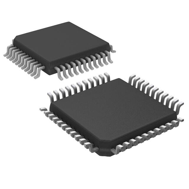
7
Package Outlines
•
P-MQFP-44
(Plastic Metric Quad Flat Package)
Sorts of Packing
Package outlines for tubes, trays etc. are contained in our
Dimensions in mm
SMD = Surface Mounted Device
Preliminary Data Sheet
30
06.99
�